

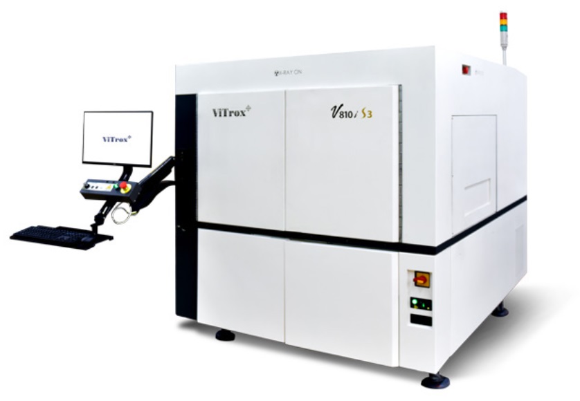
V810i S3 : Advanced 3D X-ray Inspection System (V810i S3)
Designed for various sizes of PCB assemblies to increase production efficiency and cost savings for Electronic Manufacturing Services (EMS), Original Equipment Manufacturers (OEMs), Original Design Manufacturers (ODMs), and etc.
| System | V810i S3 |
| System controller | Integrated controller with 8 Core Intel Xeon processors |
| Operating system | Windows 10 Pro (64 bit) |
| Test Development Environment | |
| User interface | Microsoft Windows based software solution with easy-to-use GUI and password-protected user levels |
| Off-line test development software | Optional for off-line PC |
| CAD conversion tool | Support 4 different types of CAD in V810i software and optional software available to translate other CAD data to ViTrox's format |
| Typical test development time | 4 hours to 1.5 days to convert raw CAD file and develop application |
| Line Integration | |
| Transport heights | 865mm-1025mm |
| Line communication standard | SMEMA, HERMES |
| Barcode readers | Compatible with most industry standard barcode readers |
| Performance Parameters * | |
| False Call rate | 500-1000ppm |
| Minimum features detection capability | |
| Joint pitch1 | 0.3mm and above |
| Short width2 | 0.045mm |
| Solder thickness | 0.0127mm |
| Allowable Panel Characteristics ** | V810i S3 |
| Maximum PCB Size (L x W) | 725mmx482.6mm (28.5"x19") |
| Minimum PCB Size (L x W) | 63.5mmx63.5mm (2.5"x 2.5") |
| Maximum PCB inspectable area | 725mmx474.9mm (28.5"x18.7") |
| Maximum PCB thickness | 7mm (276 mils) |
| Minimum PCB thickness | 0.5mm (20 mils) |
| PCB warp | Downside < 3.3mm; Upside < 3.3mm |
| Maximum PCB weight | 4.5kg |
| Top Clearance of PCB | 50mm @ 22¦Ěm resolution 42mm @ 19¦Ěm resolution 26mm @ 15¦Ěm resolution 11mm @ 12¦Ěm resolution 26mm @ 10¦Ěm resolution 11mm @ 7¦Ěm resolution (calculated from board top surface) |
| Bottom Clearance of PCB | 80mm |
| PCB edge clearance | 3mm |
| 100% Press-fit testability | Yes (With PSP2 / PSP2.1 feature) |
| PCB Temperature | 40ˇć |
| Installation Specification | |
| Power Supplies | 200¨C240 VAC three phase; 380¨C415 VAC three phase wye (+/- 5) (50Hz or 60Hz) |
| Air requirement | 552kPA (80psi) compressed air |
| System footprint (Width X Depth X Height) | 1835mmx2185mmx2162mm |
| Total system weight | ~4800kgs |
| **Note: 1. Panels are handled on width edges. Panels with edge cut outs may require the use of a carrier. 2. Maximum panel size dimensions and weight must include carrier if applicable. 3. Smaller panels are possible with the use of panel carriers. 4. With panels of this thickness, imaging results can be affected by PCBA layout. 5. Measured from the bottom of the panel including a maximum warp. *Note: 1. Assuming pad width is 50% of pitch. 2. The reported values for minimum feature detection assume that the feature is in a single plane of focus and that there are no X-ray absorbers in the X-ray path or in the immediate area of the feature other than those found in a typical multi-layer printed circuit board. #2x2 binning camera configuration. Hardware upgrade is required on old system. | |